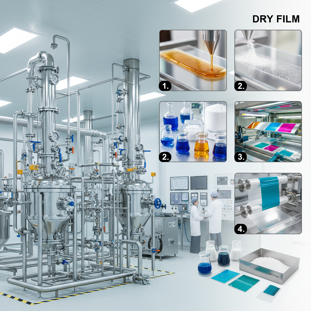
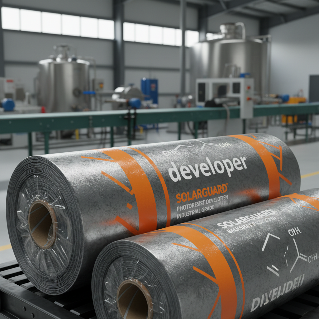
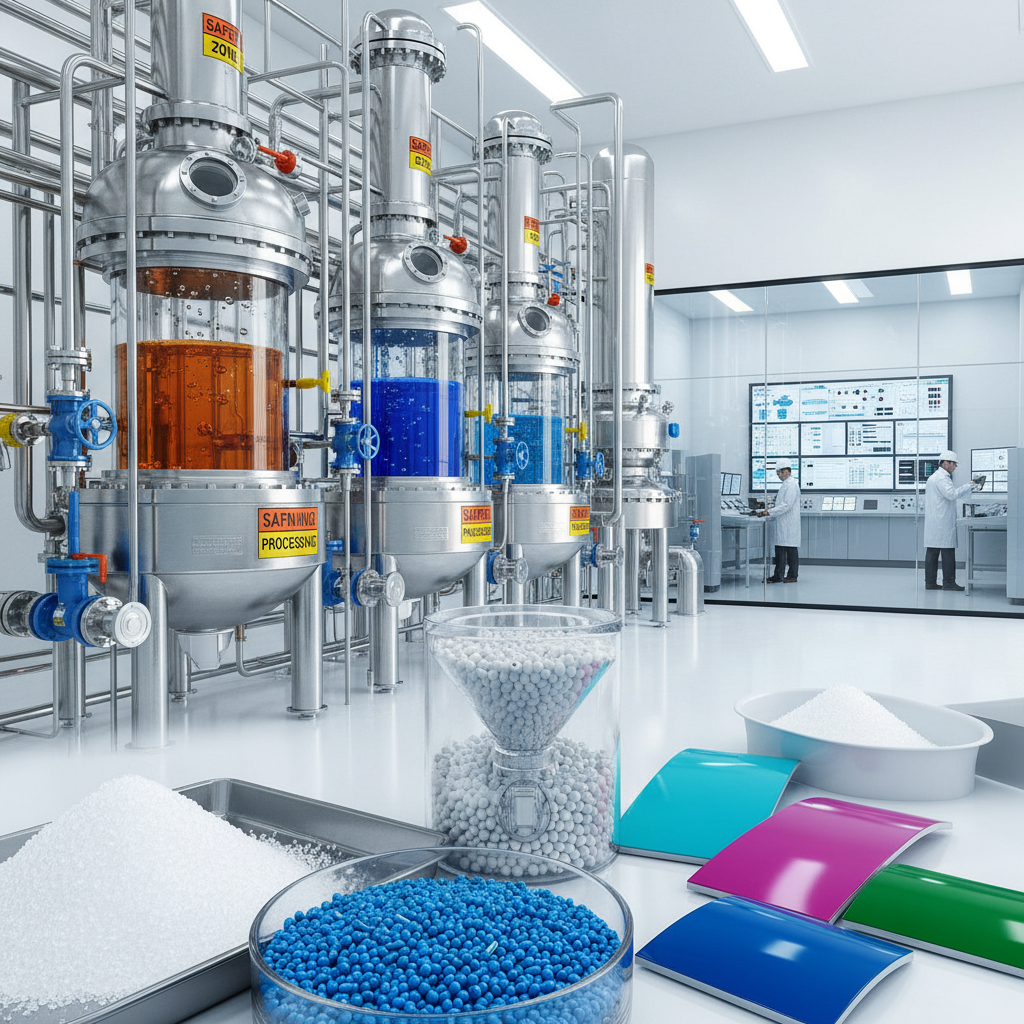
In the rapidly evolving landscape of high-precision manufacturing, dry film has emerged as a cornerstone technology for creating intricate circuitry and specialized imaging layers. By bridging the gap between liquid photoresists and solid-state masks, this innovative material allows for unparalleled precision in etching and patterning, which is essential for the modern electronics and medical device industries.
The global demand for miniaturization in electronics—from smartphones to advanced medical imaging—has pushed the boundaries of what traditional materials can achieve. The adoption of dry film resists provides a streamlined, waste-reducing alternative that enhances yield rates and ensures consistent quality across mass-production lines.
Understanding the nuances of this technology is not merely a technical requirement but a strategic advantage. As industries shift toward greener chemistry and more sustainable fabrication processes, the evolution of dry film technology continues to drive innovation in imaging information materials, medical-grade sensors, and photovoltaic energy capture.
Global Industry Context of Dry Film
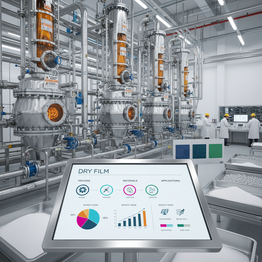
On a global scale, the shift toward Industry 4.0 has necessitated materials that can support automated, high-speed production without sacrificing micron-level accuracy. The dry film market has expanded significantly as ISO standards for electronic components have become more stringent, requiring lower defect rates and higher reliability in extreme environments.
Current statistics indicate a steady rise in the integration of photolithography materials within the Asia-Pacific and North American markets. The primary challenge addressed by this technology is the volatility and waste associated with liquid resists; by providing a pre-measured, stable layer, manufacturers can drastically reduce chemical runoff and operational downtime.
Defining Dry Film and Its Industrial Role
In simple terms, dry film is a light-sensitive polymer layer protected by a plastic carrier, designed to be laminated onto a substrate. Once exposed to UV light through a mask, the film hardens in specific areas, allowing the unexposed sections to be washed away, thereby creating a precise protective stencil for etching or plating processes.
Its connection to modern industry is profound, especially in the production of Flexible Printed Circuits (FPC) and medical diagnostic tools. Unlike wet processes, this "dry" approach eliminates the need for spin-coating and long drying times, making it the gold standard for efficiency in high-volume manufacturing of imaging information materials.
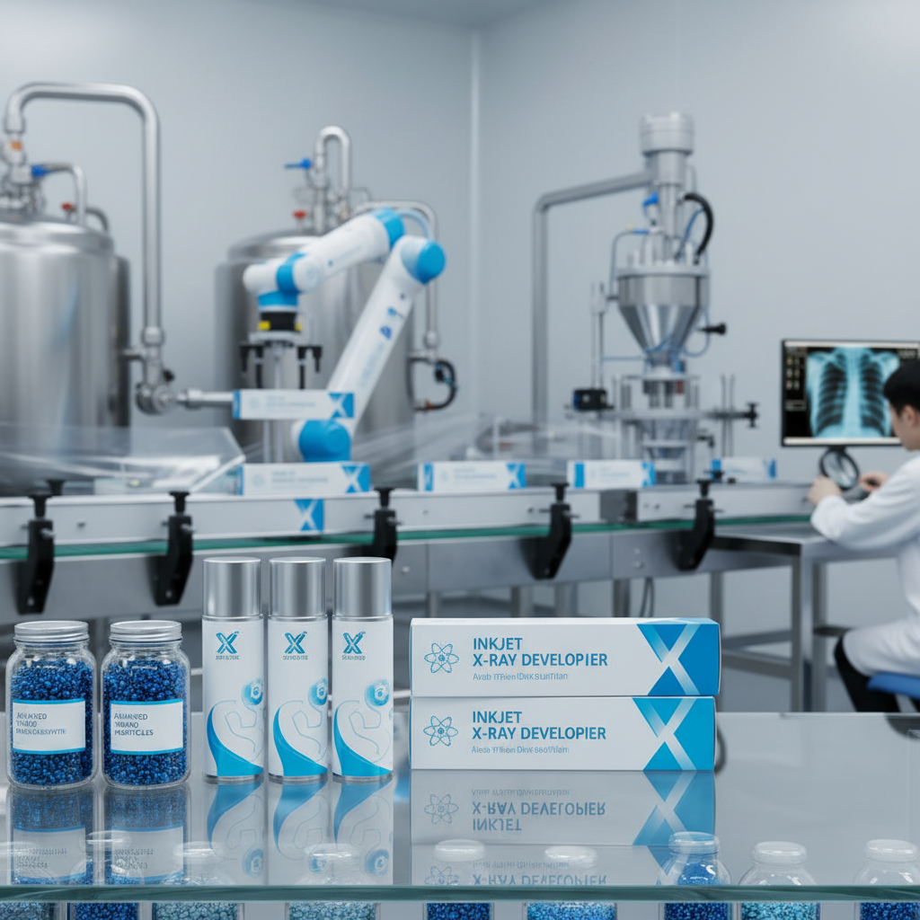
Beyond electronics, it serves humanitarian and medical needs by enabling the mass production of affordable, high-precision biosensors and imaging plates. By reducing the cost of fabrication, dry film technology helps bring life-saving diagnostic hardware to remote regions where expensive laboratory equipment is unavailable.
Core Components and Technical Factors
The efficacy of dry film depends heavily on its photochemical sensitivity. The ability of the polymer to react uniformly to UV light determines the sharpness of the edges in the final circuit, which is critical for high-frequency signal transmission in 5G hardware.
Another vital factor is adhesion strength. For the film to be effective, it must bond securely to various substrates—be it copper, glass, or specialized plastics—to prevent "undercutting" during the chemical etching phase. This ensures that the final product maintains its structural integrity under thermal stress.
Finally, process scalability and cost efficiency play a massive role. Because dry film is supplied in rolls and applied via lamination, it allows manufacturers to scale from prototype to million-unit production with minimal adjustments to the workflow, reducing the overall cost per unit.
Global Applications and Use Cases
In real-world contexts, dry film is indispensable in the aerospace industry, where lightweight, flexible circuits are required to navigate the complex geometries of aircraft wings and satellite components. In these high-stakes environments, the reliability of the resist layer prevents catastrophic failures in circuitry.
Furthermore, in the field of photovoltaic materials, this technology is used to create the fine-grid metallic lines on solar cells. By optimizing light capture and electron flow, dry film helps increase the energy conversion efficiency of solar panels deployed in massive arrays across the Sahara or the Gobi Desert.
Performance Analysis of Dry Film Application Methods
Long-Term Value and Tangible Advantages
The shift toward dry film offers a compelling logical angle: the drastic reduction in hazardous waste. By eliminating the need for solvent-heavy liquid resists, companies not only comply with environmental regulations but also lower their long-term disposal costs, creating a sustainable synergy between profit and planet.
Emotionally, the adoption of these materials builds trust with end-users. Whether it is a medical implant or a critical automotive sensor, the consistency provided by dry film ensures safety and reliability. This innovation provides peace of mind, knowing that the invisible layers of a device are engineered to the highest possible standard of precision.
Future Trends and Material Innovations
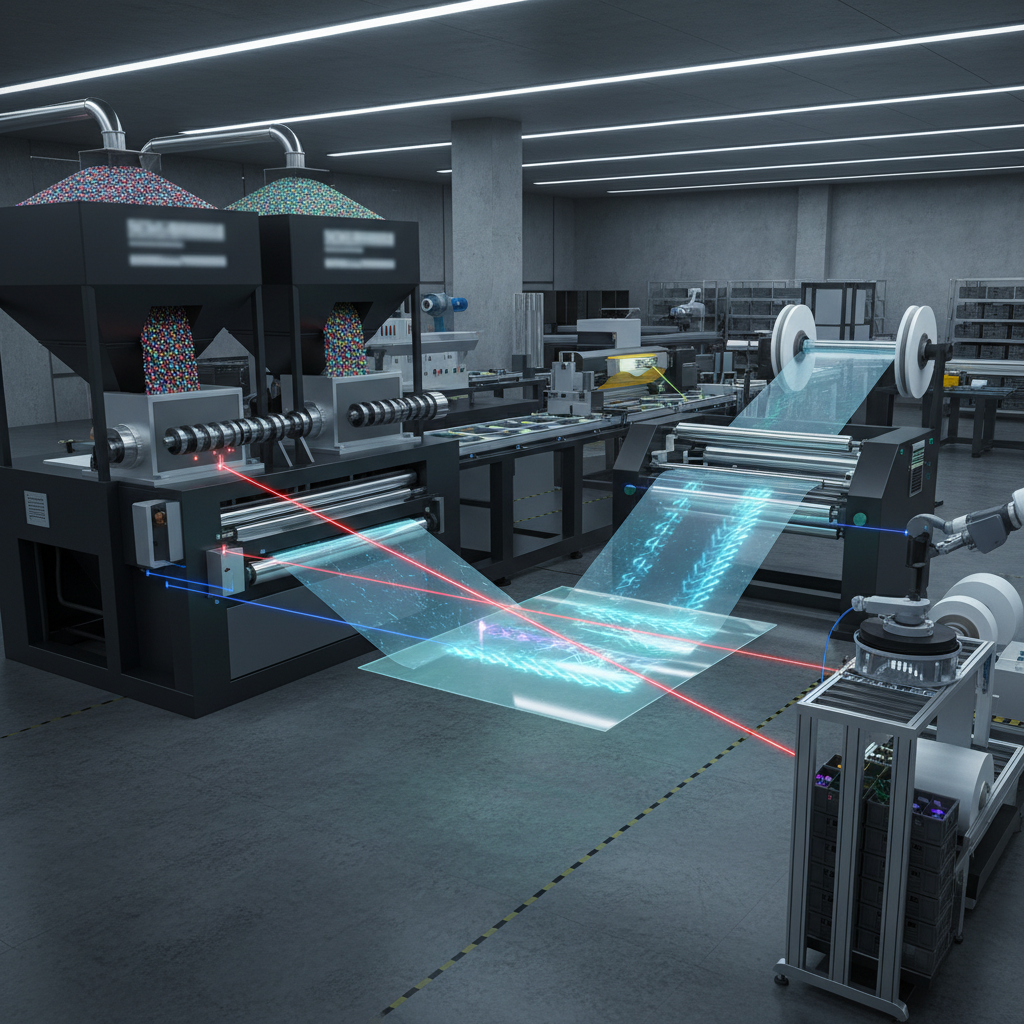
Looking ahead, the integration of digital transformation is bringing "Smart dry film" to the forefront. This involves the use of AI-driven optical inspection systems that can detect anomalies in the film thickness in real-time, allowing for automated adjustments during the lamination process to eliminate defects before they occur.
Sustainability is also driving the development of biodegradable carriers and water-soluble polymers. Future iterations of these materials aim to completely remove the need for caustic developers, moving toward a "green lithography" model that aligns with global carbon neutrality goals and circular economy principles.
Furthermore, the rise of flexible electronics—such as wearable health monitors and foldable displays—is pushing dry film toward higher elasticity. New hybrid organic-inorganic materials are being tested to ensure that the resist layer can withstand repeated bending without cracking or peeling.
Overcoming Technical Challenges in Implementation
Despite its advantages, dry film implementation is not without challenges. One of the most common issues is the formation of air bubbles or "voids" during lamination, which can lead to broken circuits. This is typically solved by implementing vacuum lamination systems and strict temperature controls to ensure a seamless bond.
Another hurdle is the sensitivity to storage conditions; temperature and humidity fluctuations can cause the film to degrade before use. Expert insights suggest the use of climate-controlled "cold chain" storage and the implementation of First-In-First-Out (FIFO) inventory management to maintain optimal chemical activity.
Finally, the balance between resolution and throughput can be difficult. While slower exposure times increase precision, they lower productivity. The solution lies in the adoption of high-intensity LED UV curing systems, which provide the necessary energy for sharp definition while significantly accelerating the production cycle.
Comparative Analysis of Dry Film Technical Specifications
| Material Grade |
Resolution (μm) |
Adhesion Score (1-10) |
Application Focus |
| Standard Industrial |
25-50 |
7 |
General PCB |
| High-Precision Medical |
5-10 |
9 |
Bio-Sensors |
| Ultra-Thin Flex |
15-20 |
8 |
FPC / Wearables |
| Photovoltaic Grade |
30-60 |
6 |
Solar Grid Lines |
| Aerospace Spec |
10-15 |
10 |
Satellite Avionics |
| Eco-Friendly Hybrid |
20-40 |
7 |
Sustainable Tech |
FAQS
Dry film eliminates the need for spin-coating and baking, which significantly reduces production time and chemical waste. It ensures a perfectly uniform thickness across the entire substrate, leading to higher consistency and fewer defects compared to liquid resists, which can suffer from edge-bead effects and uneven drying.
Because dry film contains light-sensitive polymers, exposure to heat or stray UV light can cause premature polymerization. Storing the material in a cold, dark environment (typically 2-8°C) prevents degradation, ensuring that the film reacts precisely during the actual exposure process to maintain high resolution.
Yes, provided the surface is properly treated. By using specialized adhesion promoters or plasma treatment, dry film can bond effectively to glass for MEMS devices or plastics for flexible electronics. The key is matching the polymer chemistry of the film to the surface energy of the substrate.
Lifting usually occurs due to poor adhesion or inadequate UV exposure. If the film is not fully cured or if there is contamination on the substrate, the etching chemicals can seep under the resist. This is solved by optimizing exposure doses and ensuring a rigorous surface cleaning process before lamination.
Absolutely. Modern dry film trends are moving toward water-developable resists and biodegradable carrier sheets. By reducing the reliance on organic solvents and cutting down on the volume of waste chemicals, manufacturers can significantly lower their environmental footprint while maintaining industrial performance.
The thickness should be determined by the required etching depth and the thickness of the material being removed. A thicker film provides better protection for deep etches but may reduce the resolution of very fine lines. Consulting a technical data sheet and performing a step-wedge test is recommended to find the optimal balance.
Conclusion
In summary, dry film represents a critical evolution in material science, providing the precision, scalability, and reliability required for today's most demanding industrial applications. From the intricate layers of medical sensors to the massive grids of photovoltaic panels, its ability to deliver consistent, high-resolution patterning while reducing environmental impact makes it an indispensable tool for modern manufacturing.
As we move toward a future defined by flexible electronics and sustainable production, the continued innovation of photolithography materials will be key to unlocking new technological possibilities. We encourage engineers and procurement specialists to explore advanced film specifications to optimize their yields and reduce operational costs. Visit our website: www.lkintl.com